|
While doing the PCB layout stuff for the SDrive NUXX, I’ve spent a lot of time trying to make the traces as simple and attractive as possible, while ensuring the components on the PCB are reasonably well spaced and thus easy for an average DIY person to solder. When I do this, I set up the board with two layers, with the top primarily being the ground plane, and the bottom holding as many of the other connections as possible.
After establishing part footprints and placement (mostly based on front / rear panel controls in the SDrive NUXX’s case) I then try to lay out the rest of the parts, fitting them together like Lego, taking into account things that need to be near each other (caps and certain things), and other stuff like that. Then I route the board, trying to keep as many traces on the bottom as possible and moving repositionable components as needed. Of course, surface mount parts often require their traces to be on the top, but generally most things can be kept on the bottom.
Once everything connected in a layout that is looking good I’ll turn off everything but the top and bottom layers and associated pads, vias, and airwires. I then look at every top layer trace, and if it’s not needed for an SMT part or crossing over a trace on the bottom, I’ll try to move it to the bottom.
Next I’ll turn alternate showing only the top or bottom layers, as shown above. On the left is the top (or component) side with its traces in red, and on the right is the bottom (or solder) side in blue. Looking at just one side at a time I can more easily see traces routed in unnecessarily complex patterns. Sometimes I’ll have stairstepped a trace or routed it around something when a much simpler, straighter path would do. I find that having more layers (documentation, part outlines, part names, etc) turned on while doing hand-optimizing causes me to keep traces of areas where they can safely go, particularly under other components. Hiding this information clutter lets me focus on the bare wiring itself making the task even easier.
After a few rounds of this I generally find that the result is a layout with simple, direct, and well organized traces.

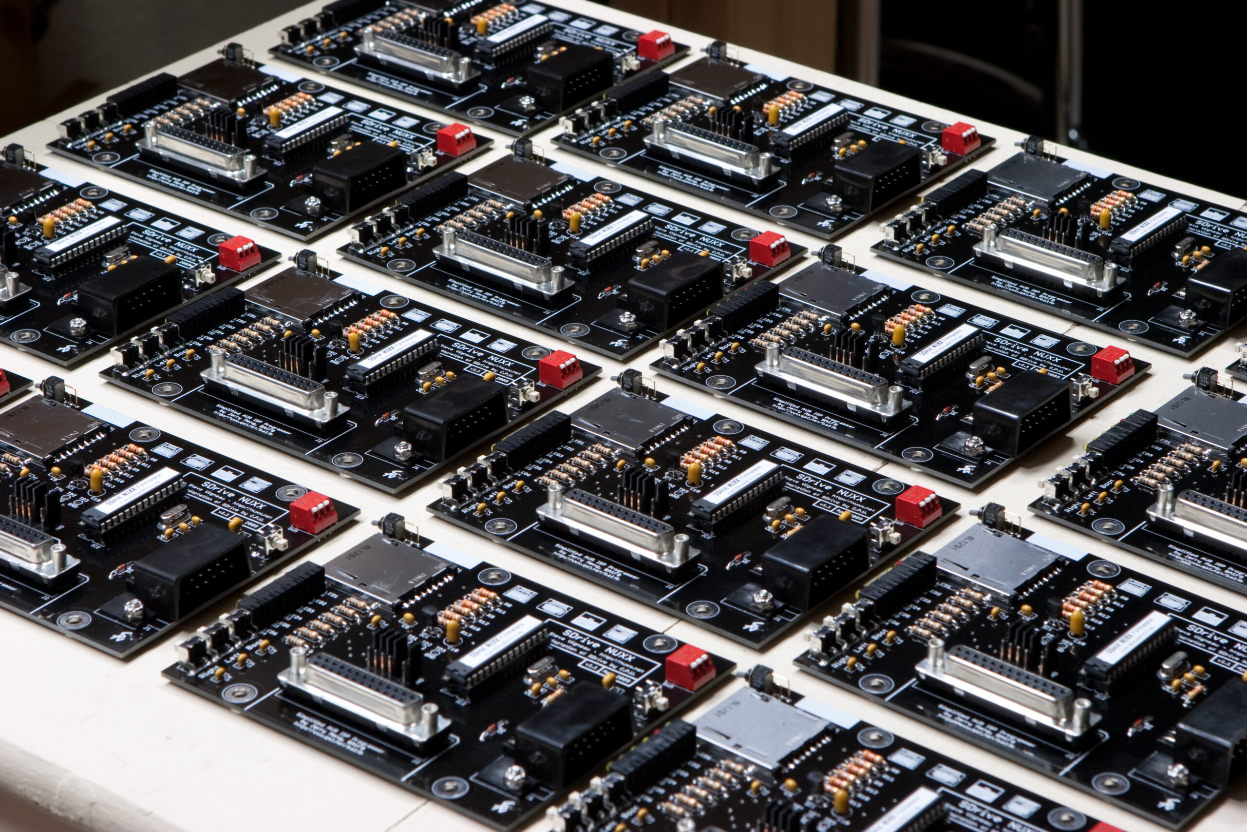
Buying twelve SD cards at a time feels a bit odd. However, they are needed, as the assembled SDrive NUXXs each come with one. They’ve all now been reformatted as FAT, labeled (SDRIVE_NUXX), and had SDRIVE.ATR copied to the root. Checksums were done to ensure that the file arrived intact.
I’ve also got a line on some more SIO connectors, so it’s possible I’ll be able to open up the ordering further than I had before. Being able to do this would be good, as I’ve already got a couple people on the wait list.

It’s happened. The SDrive NUXX parts are finally available for ordering over on the SDrive NUXX Ordering Page. As noted here on the AtariAge forum I’ve got four things for sale:
· SDrive NUXX PCB & End Panel Set – US$35 – One SDrive NUXX PCB v1.1, one set (front and rear) SDrive NUXX End Panels, two thread-cutting screws for mounting thick-wing SIO connectors, and two 4-40 screw/nut sets for mounting thin-wing SIO connectors.
· Preprogrammed Microcontroller – US$5 – One Atmega ATmega8-16PU (PDIP28 package) microcontroller, programmed with the SDrive firmware with the Brown-Out Detection (BODEN and BODLEVEL) fuses programmed. Only available with the purchase of an SDrive NUXX PCB & End Panel Set or SDrive NUXX Kit.
· SDrive NUXX Kit – US$100 – The aforementioned PCB & End Panel Set, plus a preprogrammed Atmel ATmega8 microcontroller, and all the other parts for building one SDrive NUXX except for an SIO connector. This includes a black Hammond Manufacturing 1455L1201BK enclosure. Note that if you wish to use the enclosed DB15 connector instead of your own SIO connector, some slight modification of the IO Connector hole on the rear panel will be required to ensure that the mounting screws fit.
· Completely Assembled and Tested SDrive NUXX – US$150 – One completely assembled SDrive NUXX with SIO connector, tested and ready to use. Includes a 2GB Kingston SD card containing SDRIVE.ATR, tested to work with the SDrive NUXX. As I only have access to a limited number of SIO connectors, this is limited to a total of 10 items, to be sold on a first-come, first-served basis.
All aforementioned items ship FOR FREE via First-Class Mail to US addresses. For international destinations, postage (via First-Class Mail) is a flat-rate US$7 to international destinations for each complete SDrive NUXX, SDrive NUXX Kit, or every five SDrive NUXX PCB & End Panel sets.
From now through 03-April-2009 I will be accepting orders. After 03-April-2009 the ordering window will be closed and I will begin ordering the parts. The PCB and end panel manufacturers have quoted me three weeks lead time for manufacturing, and then a week (or so) for shipping, meaning that I should receive these parts around the beginning of May. As soon as the PCBs and end panels are received I will begin assembling and shipping orders. I will have all orders shipped out as soon as possible.
So, that said, if you’d like to place an order, please head on over to the SDrive NUXX Ordering Page. The payments are handled via Google Checkout. Note that if you are wanting to order an assembled SDrive NUXX (or get on the waiting list for in the case that ordering is full) an assembled SDrive NUXX you will need to email me directly. (See the ordering page for more information on this.)
And, finally, please be sure to review the SDrive NUXX, SDrive, and SDrive NUXX Ordering pages before ordering, to ensure that you have a good understanding of what it is that you are buying. This is a DIY project, and while all parts are guaranteed to be free from defects they are otherwise without warranty or technical support.

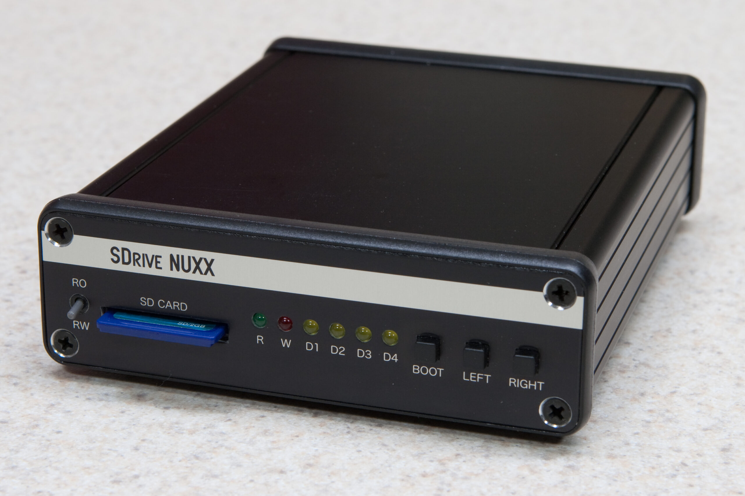
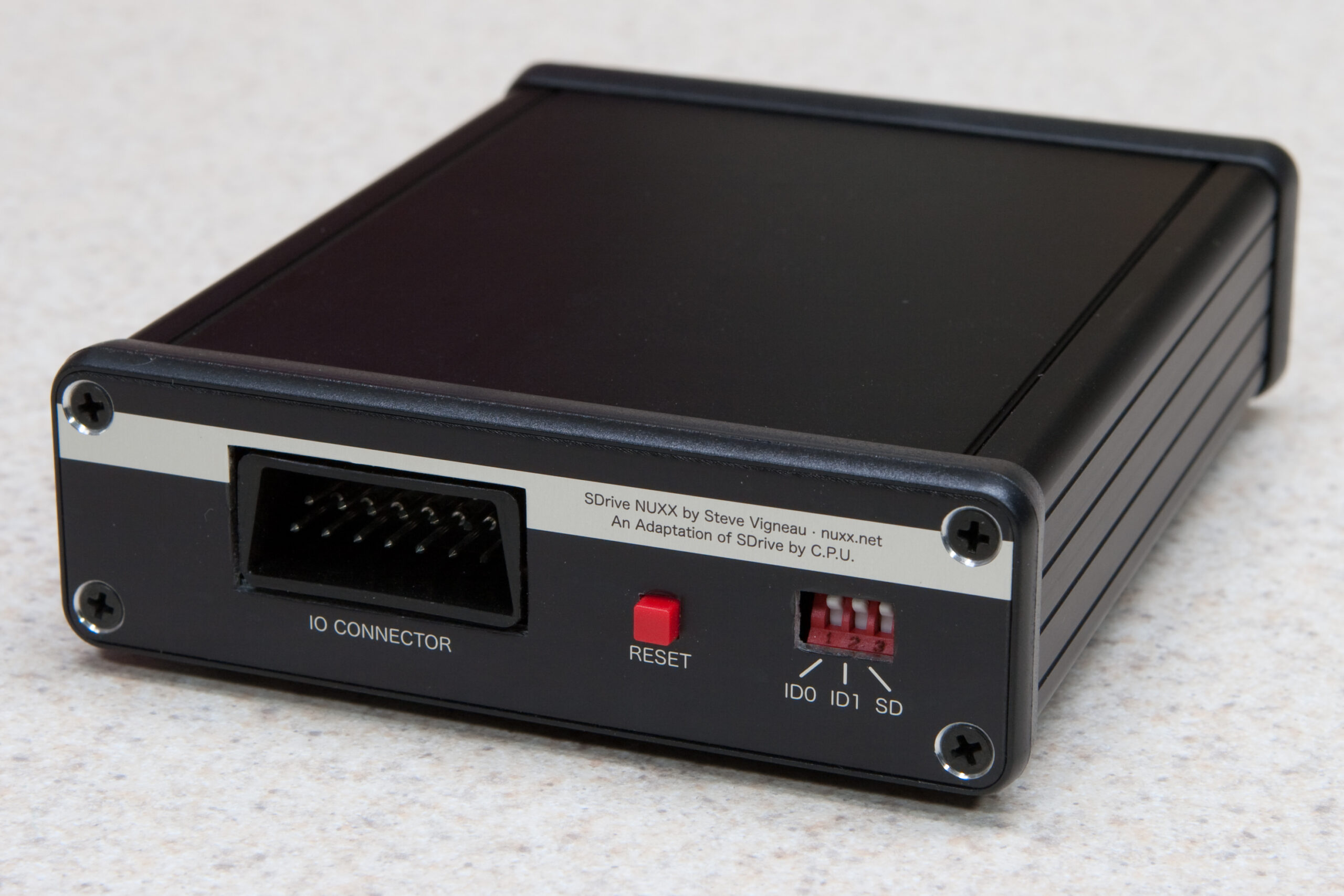
After a very busy weekend working on polishing the SDrive NUXX documentation, PCB layout, end panel artwork, and programming nuances (in between fun times for dinner with friends, parents visiting for dinner, etc) I’ve come to what I hope are the final versions. That up there is v1.0 of the end panels, which I hope capture a nice 80s feel with the Atari-esque font for the name and the round-end single-pass-with-a-cutter-in-a-mill line font for the labels.
This artwork is also (hopefully) much better than the last stuff I posted, a bit over a month ago, which was rather limited, particularly due to the limited features of Front Panel Designer. This new artwork was done in Illustrator, providing far, far more flexibility. Hopefully the end panels will come out nicely.
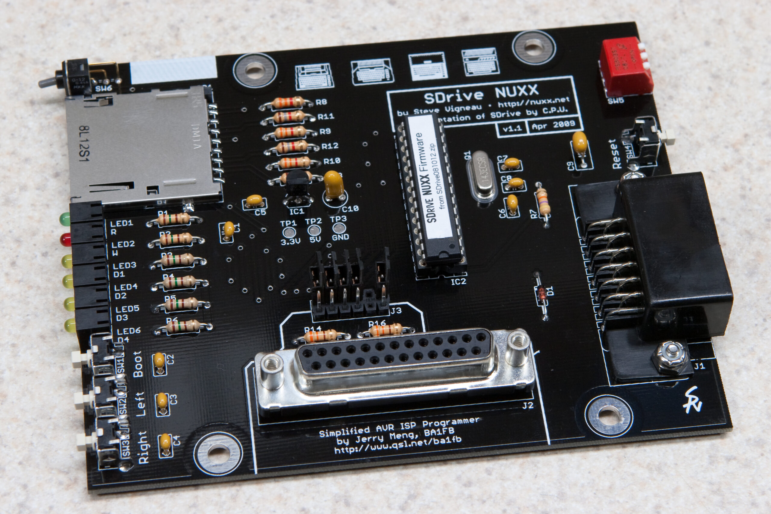
I’ve also finished off v1.1 of the PCBs, moving the tactile switches slightly outwards, adding two missing traces, fixing a footprint, and adding test pads to make voltage testing after assembly easier. This, combined with the finished artwork, and the (forthcoming) results of kurtm‘s testing will hopefully allow me to open up ordering by Wednesday. Yay! Now it’s time to rest for a day or three.
|