NetOptics Passive 10/100 Ethernet Port Aggregator Tap Disassembly
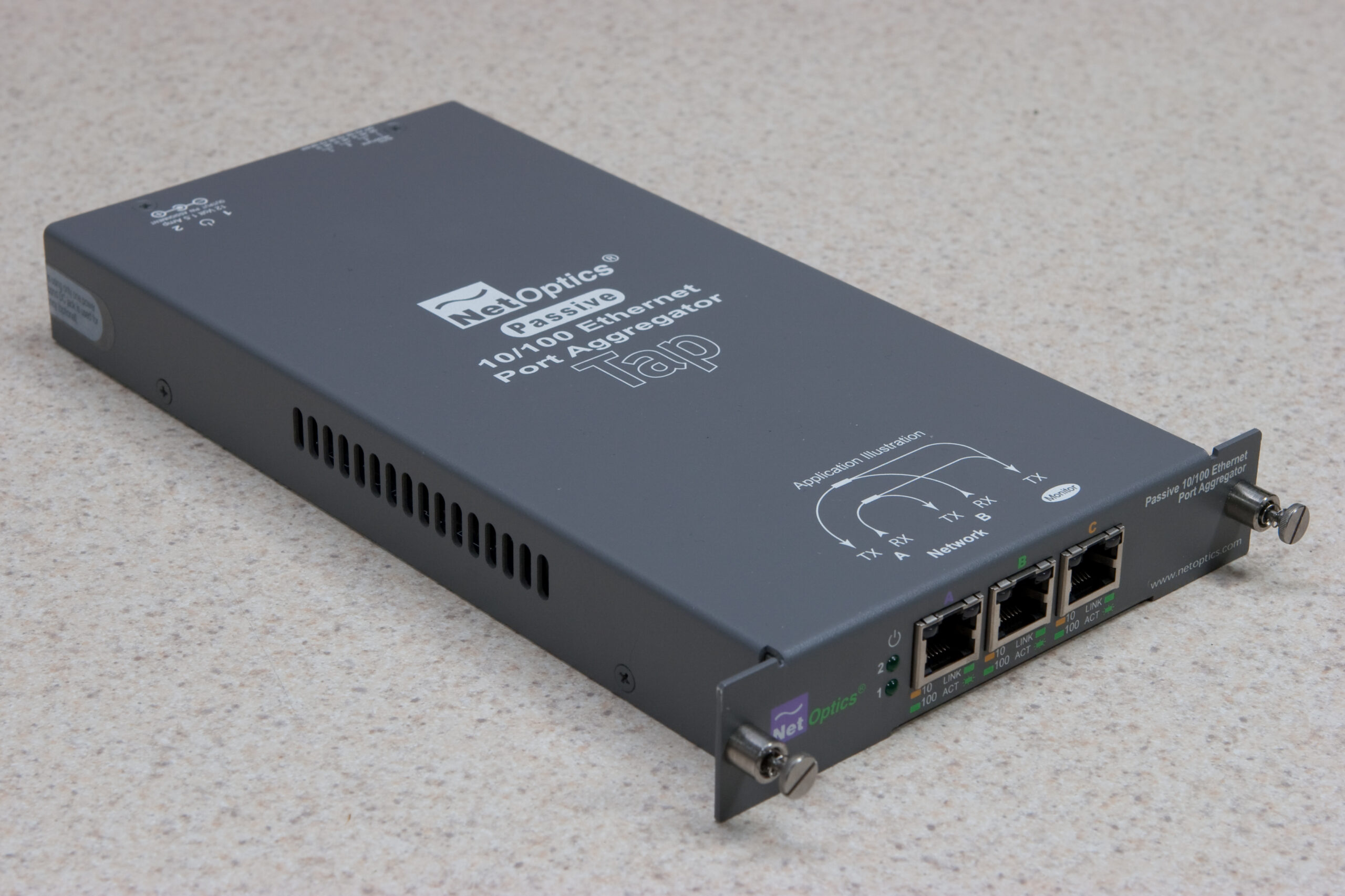
Today I received a rather nifty device, an older-model Passive 10/100 Ethernet Port Aggregator Tap (PA-CU) from NetOptics. This device allows one to monitor both halves of a full-duplex 10/100 network connection at once, with only one capture device, which is rather nifty.
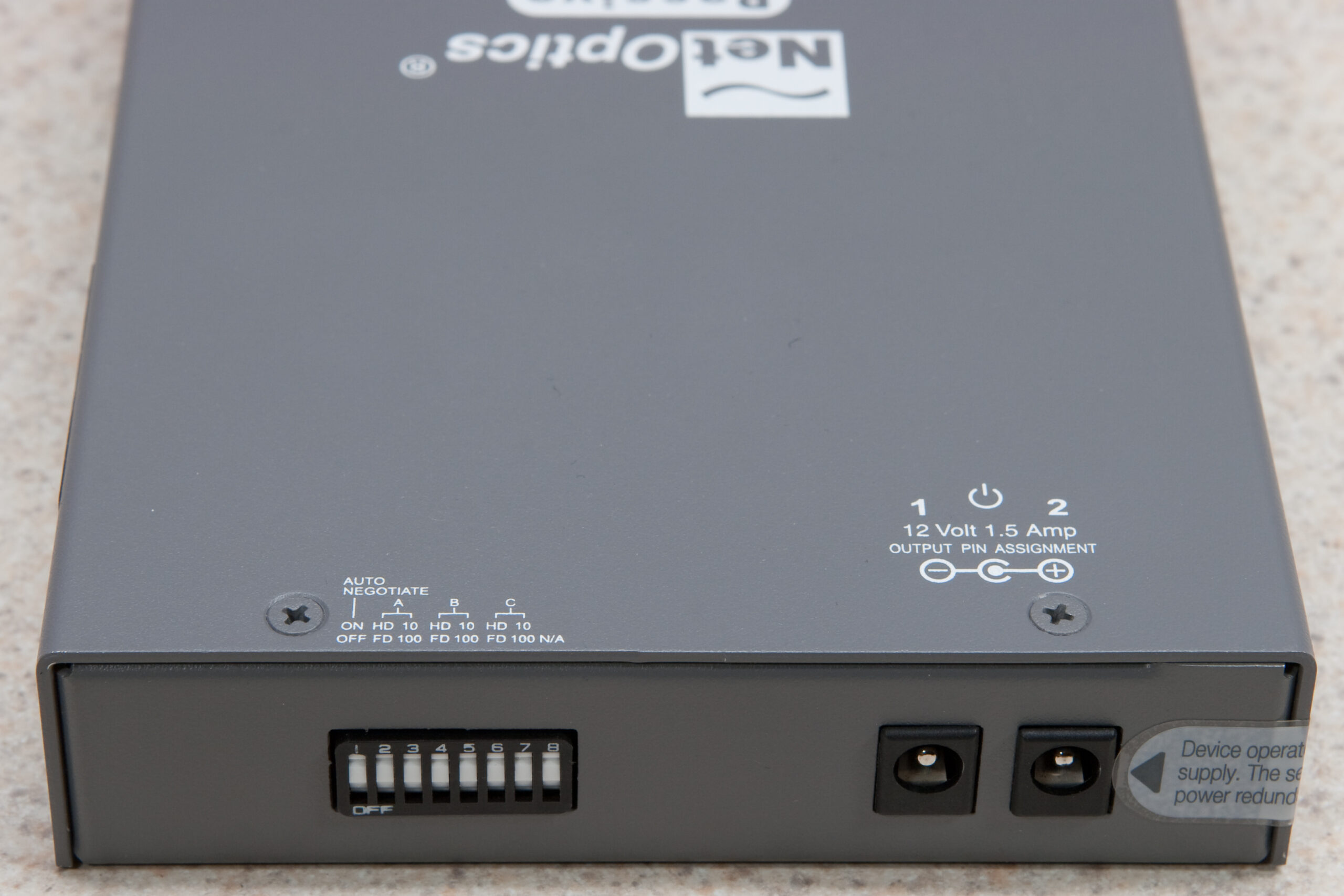
It was delivered quite early this morning by FedEx, and upon opening the box I saw that it was practically new, with the power supply shipping bags still sealed. There was no documentation, but this was easy enough to find online, and only consists of jumpers whose settings are silkscreened on the top of the enclosure.
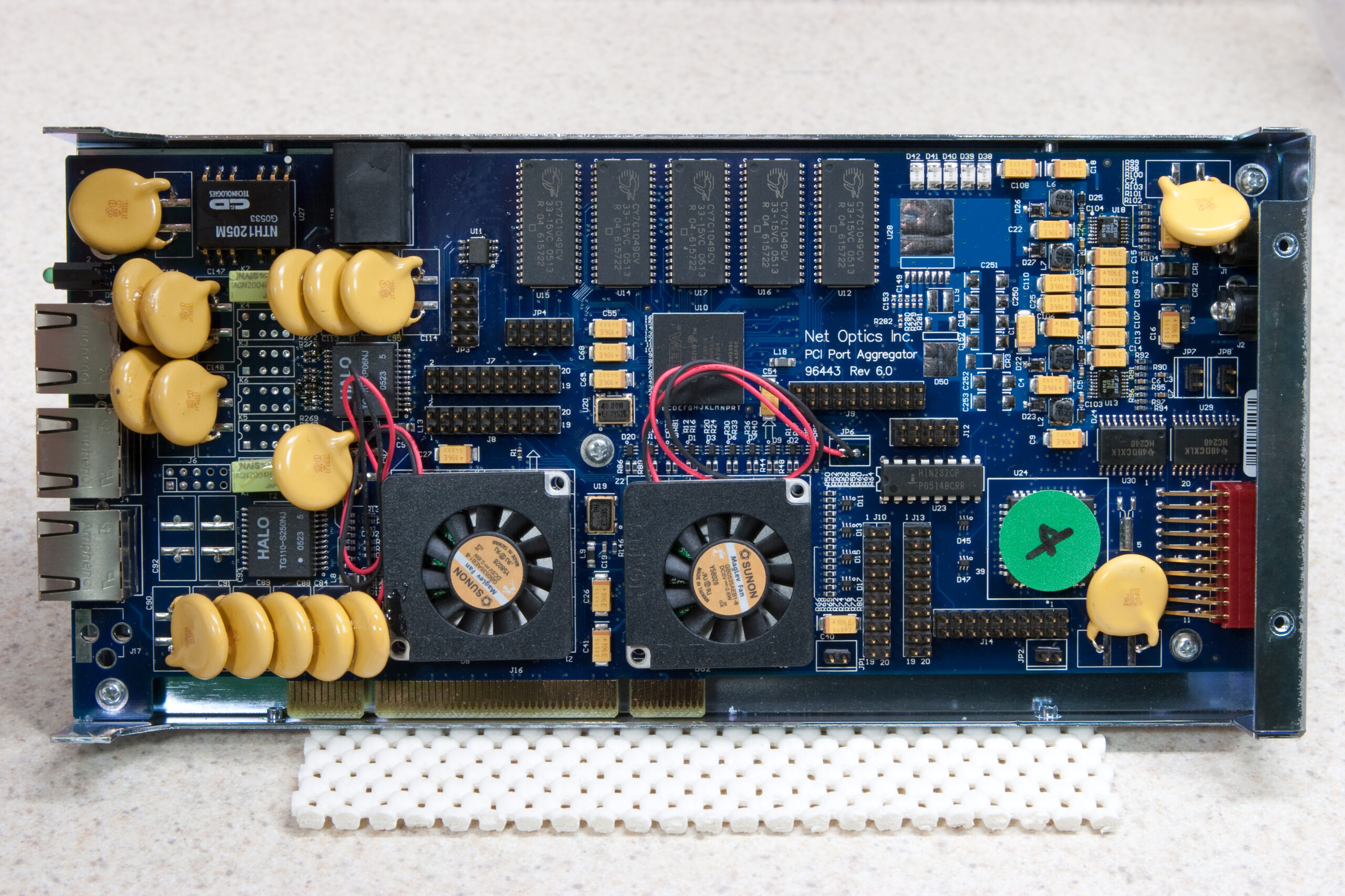
After trying it out today I decided that it would be good to open it up and see what is inside. As this photo shows it is basically their older PCI aggretator tap repackaged into a rather nice metal housing. This board contains a FPGA, a bunch of SRAM, a PIC, and some currently unidentified (but well heatsinked) processors.
If you’d like to see more photos of the inside of the tap, they are all available here: NetOptics Passive 10/100 Ethernet Port Aggregator Tap (photo gallery retired).
Hi Steve-
Nice site here! I live in the Grand Rapids, MI area, and was doing some research on the NetOptics products, which led me here. I have a couple of observations/comments regarding your internal pictures of the device here, which might be relevant due to my personal experience with FPGA development:
1.) The photo showing all the round yellow components is probably part of the power supply, because the small black chip labeled “C&D 1205M” is a 2-watt DC-to-DC converter IC.
2.) In the picture containing the PIC microcontroller, chip labeled “U23” is an Intersil RS-232 Transceiver, and the PIC18F452 is more than likely being used mostly for loading the datastream into the FPGA chip, as well as being in control of “supervisory” functions regarding power and preset operating parameters via PCB jumpers/DIP switches.
3.) Photo IMG3483 shows U13, which I believe to be a Linear Technology 1.4-amp switching regulator device. Right next to it are what I would think to be two Texas Instruments ‘HC240 Inverting-Type Octal Buffer/Driver chips.
4.) The devices located under the fans are possibly some sort of specialized network processing ASIC, maybe a LSI APP300?
5.) The ICs labeled “HALO” are surface-mount network electrical isolation devices, and are common to many Ethernet device designs.
6.) The Altera FPGA is probably providing a software-based Ethernet “PHY” for all the ports, and the Cypress SRAM is simply a network data “buffer” area for those software PHYs.
It looks like a great box, probably lots of fun to play with! Enjoy it… :)
Kindest Regards,
Cliff
Ooops, a quick correction to comment #6 above: I put Ethernet “PHY” when I really meant Ethernet “MAC” cores!
An Ethernet PHY is usually done in an IC, not in software…
Cliff