Two-Layer Simple PCB Routing
While doing the PCB layout stuff for the SDrive NUXX, I’ve spent a lot of time trying to make the traces as simple and attractive as possible, while ensuring the components on the PCB are reasonably well spaced and thus easy for an average DIY person to solder. When I do this, I set up the board with two layers, with the top primarily being the ground plane, and the bottom holding as many of the other connections as possible.
After establishing part footprints and placement (mostly based on front / rear panel controls in the SDrive NUXX’s case) I then try to lay out the rest of the parts, fitting them together like Lego, taking into account things that need to be near each other (caps and certain things), and other stuff like that. Then I route the board, trying to keep as many traces on the bottom as possible and moving repositionable components as needed. Of course, surface mount parts often require their traces to be on the top, but generally most things can be kept on the bottom.
Once everything connected in a layout that is looking good I’ll turn off everything but the top and bottom layers and associated pads, vias, and airwires. I then look at every top layer trace, and if it’s not needed for an SMT part or crossing over a trace on the bottom, I’ll try to move it to the bottom.
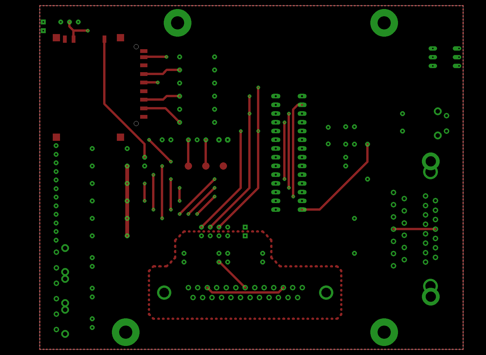
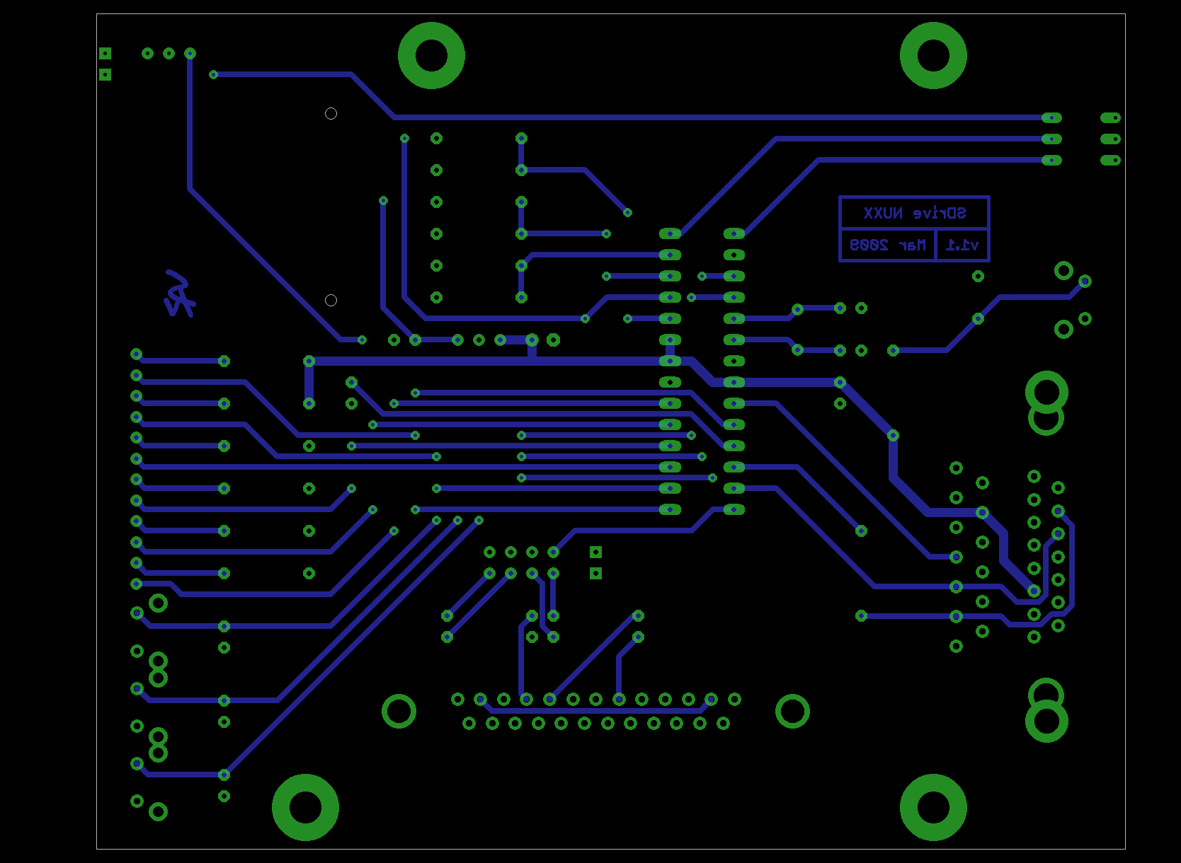
Next I’ll turn alternate showing only the top or bottom layers, as shown above. On the left is the top (or component) side with its traces in red, and on the right is the bottom (or solder) side in blue. Looking at just one side at a time I can more easily see traces routed in unnecessarily complex patterns. Sometimes I’ll have stairstepped a trace or routed it around something when a much simpler, straighter path would do. I find that having more layers (documentation, part outlines, part names, etc) turned on while doing hand-optimizing causes me to keep traces of areas where they can safely go, particularly under other components. Hiding this information clutter lets me focus on the bare wiring itself making the task even easier.
After a few rounds of this I generally find that the result is a layout with simple, direct, and well organized traces.