Healing a Hefty Scrape
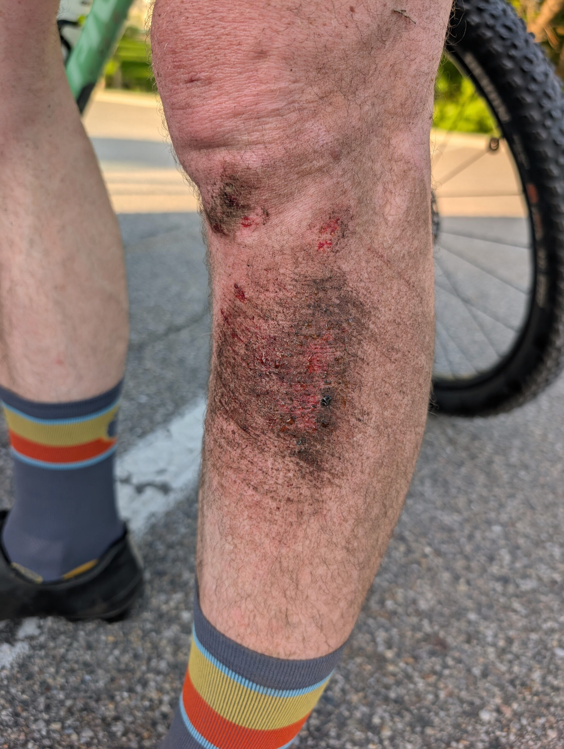
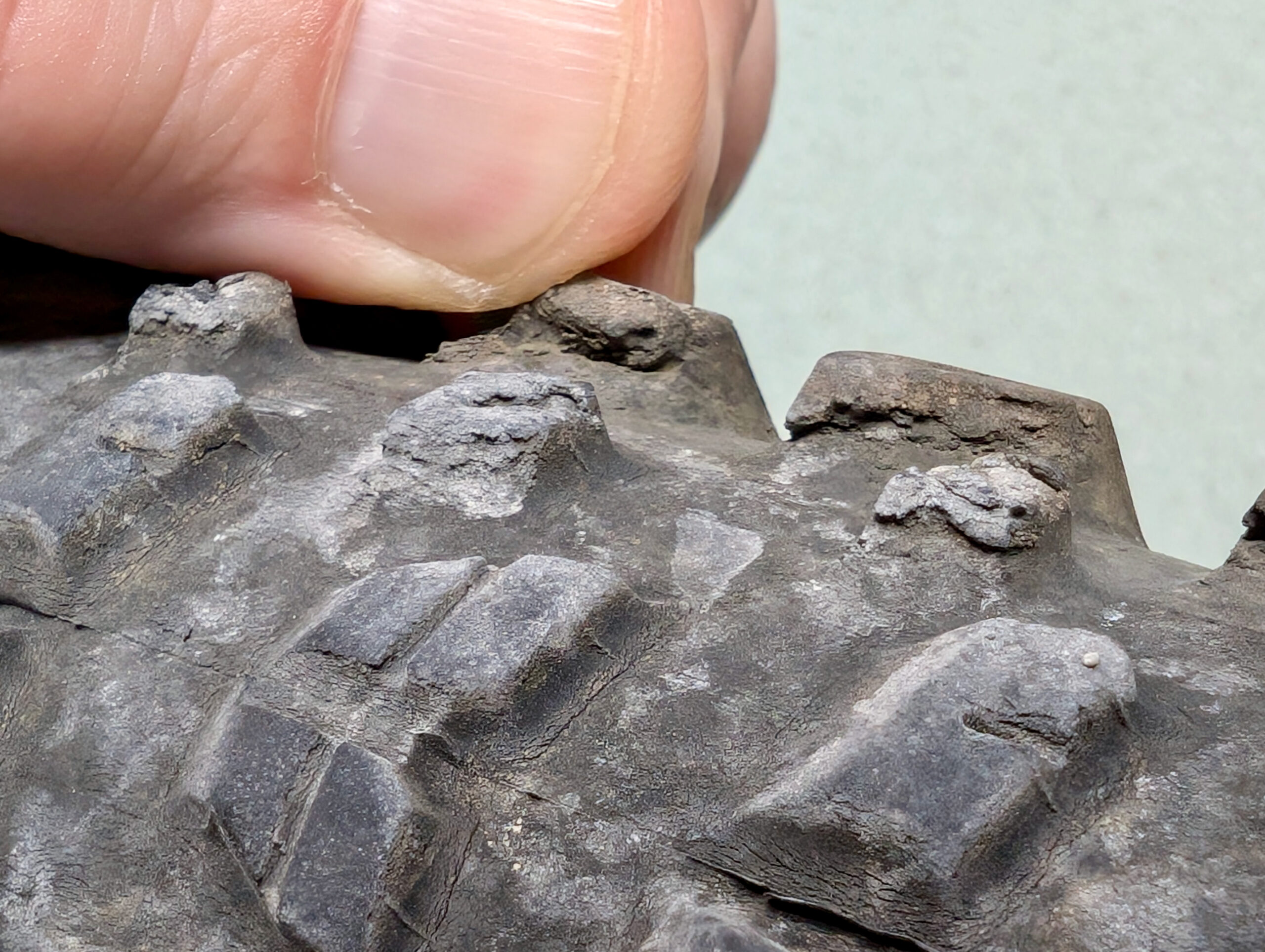
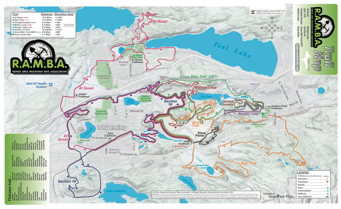
As much as I try to avoid them, I’m unfortunately familiar with the bumps and scrapes that come with mountain biking; typically minor injuries from brushing a tree of or falling over in the dirt. A few weeks back when riding at River Bends on a far-too-worn-out tire and working on faster, flat cornering, I ended up sliding out, falling over, and scraping the front / outer-side of my left shin / calf on some hard-packed sand.
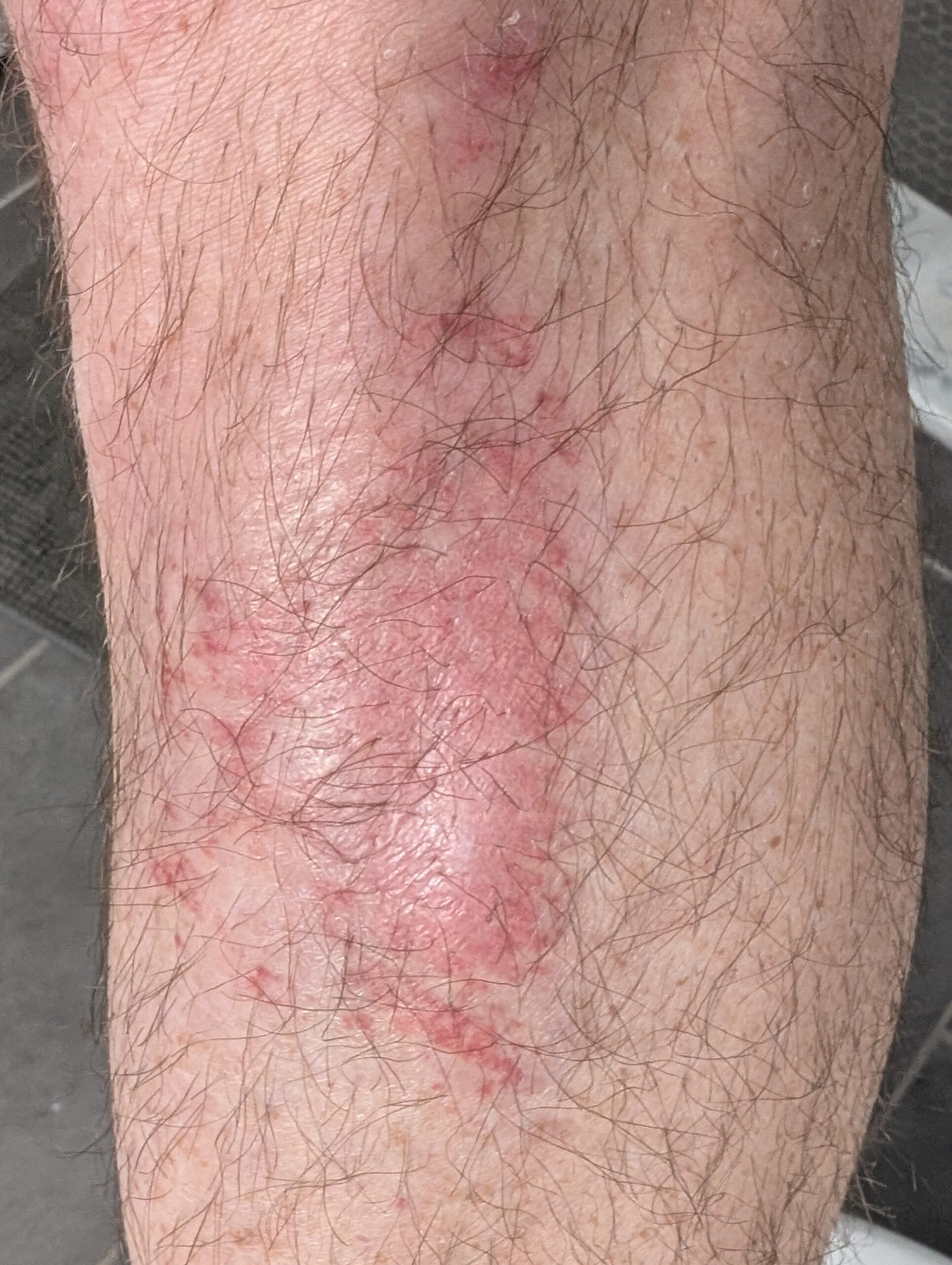
This wouldn’t have been notable at all, except it was a bit deeper than normal and thus had difficulty figuring out how to treat it. I subsequently got a (likely staph) infection that made it much more painful, and took a lot longer to heal, than a normal abrasion / road rash. Thus this post, wherein I document what went wrong, what went (very) right in healing it up, and what I intend to do next time.
What Went Right
After a week of getting worse, and a few days of constant stinging pain that even interfered with sleep, I went to urgent care because I was concerned it was getting infected. The nurse practitioner agreed that it seemed infected and prescribed cephalexin (oral) and mupirocin (topical) antibiotics. Beginning to take these cleared up the infection and allowed healing to begin.
A riding friend who noticed the bandage, and whose spouse works in wound care in an ER, had dealt with a much-worse leg injury in the past, took an interest, and the two of them recommended a course of action that worked wonderfully:
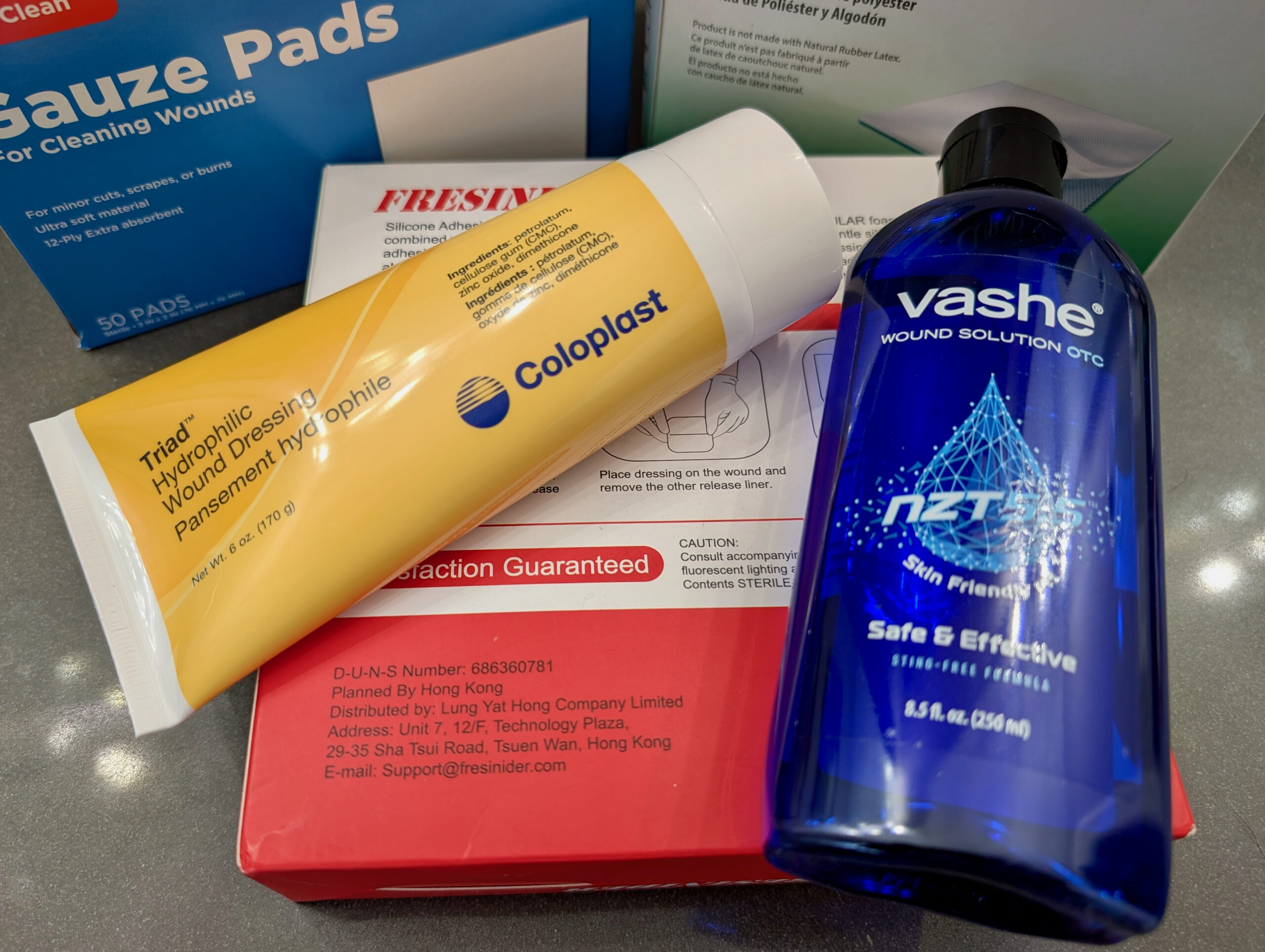
- Regularly clean the wound with Vashe Wound Solution OTC and a gauze pad, letting it soak for while.
- Cover it with mupirocin and a non-stick pad taped in place. Replace this regularly until weeping stops.
- After weeping has stopped, continue cleaning with Vashe, then cover with a thick (~2mm) layer of Triad Wound Dressing covered with a breathable foam bandage. (I used these 5″ x 5″ dressings from Amazon.)
This worked amazingly well and in about a week of Triad + breathable bandages everything was healed well enough that I no longer needed to bandage it. Three weeks after I scraped my leg — two of which were un- to counter-productive — it’s still a little pink and tender, but otherwise just looks like skin. And I’m very relieved.
What Went Wrong
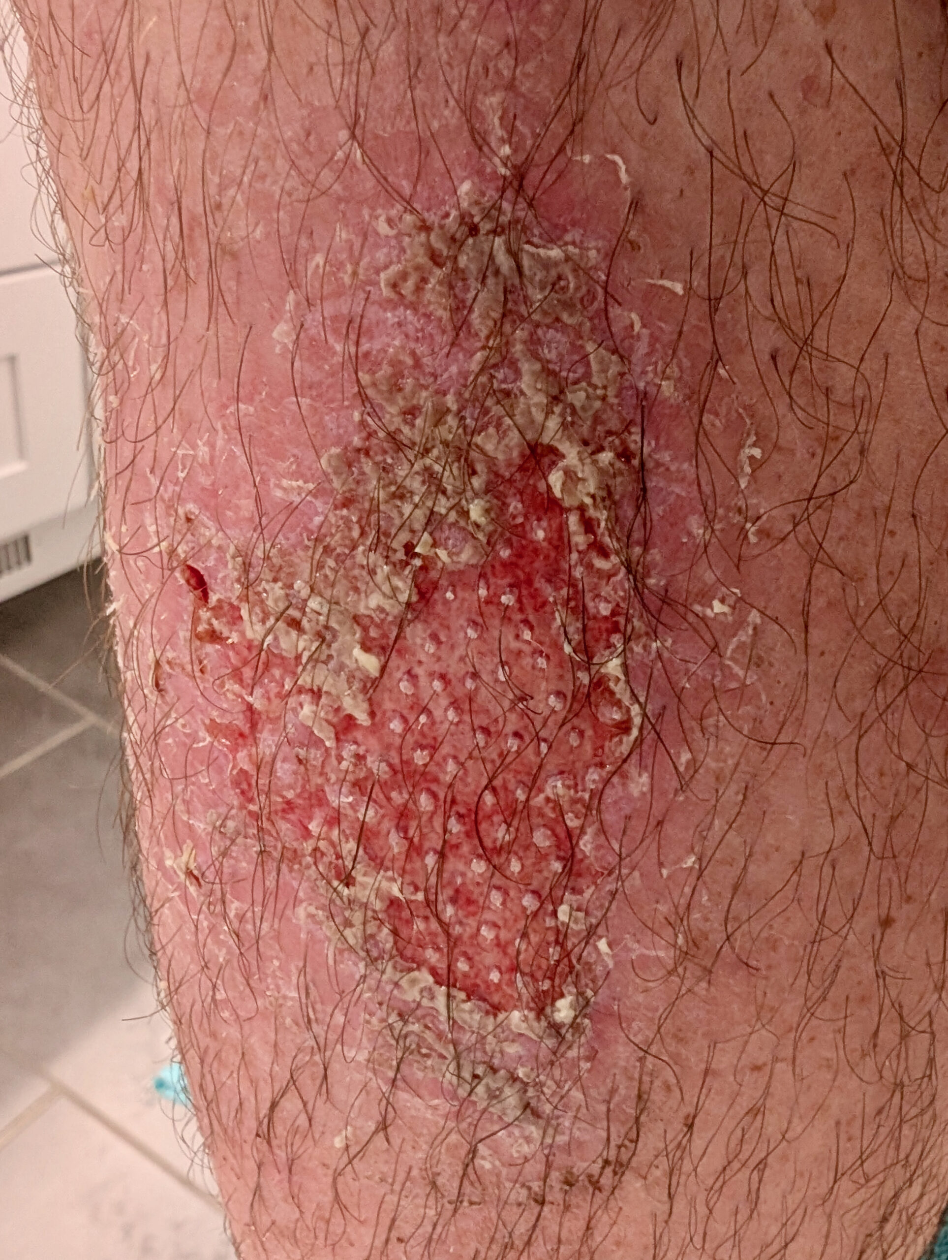
Before things went right, they went very wrong, to the point where for a three-day period it hurt constantly, akin to the washing-a-scrape-in-the-shower feeling. Ibuprofen kinda helped, but I still had difficulty sleeping and as my leg muscles would flex while standing the skin would burn and ache. While I didn’t have a fever, the infection looked scary, felt warm, and I didn’t want it to get worse.
So what shouldn’t I have done?
- Incomplete Cleaning: The first night I thought I washed the wound well enough, but the next evening I found there was still dirt mixed in with the forming scab. I’m not sure if this would have been enough, but it wouldn’t have made things worse. This is where Vashe would have come in handy.
- NEOSPORIN + Lidocaine: I’m not sure why this happened, but I figured NEOSPORIN + Lidocaine would help with the stinging. Instead it did the opposite; this made it burn worse and it took a few hours for the burning to go away.
- Hydrocolloidal Dressing: The typical cycling recommendation for abrasions seems to be Tegaderm. Hydrocollodial dressings came recommended by some friends as working for them, so I tried applying a thicker hydrocollodial dressing + NEOSPORIN for a couple days beginning three days after the injury. I don’t believe this caused the infection, but I also don’t think it helped; this time was when the infection really set in. It clearly works for some people, but I’ll avoid it next time.
Next Time
Given all this, what will I do next time?
- Wash thoroughly with soap+water, then flood/wash/soak with Vashe and re-wash similarly between dressing changes.
- Initially coat with a topical anti-microbial silver wound gel and cover with a non-stick pad held in place with tape.
- After bleeding/significant weeping stops, switch to Triad and breathable foam bandages.


